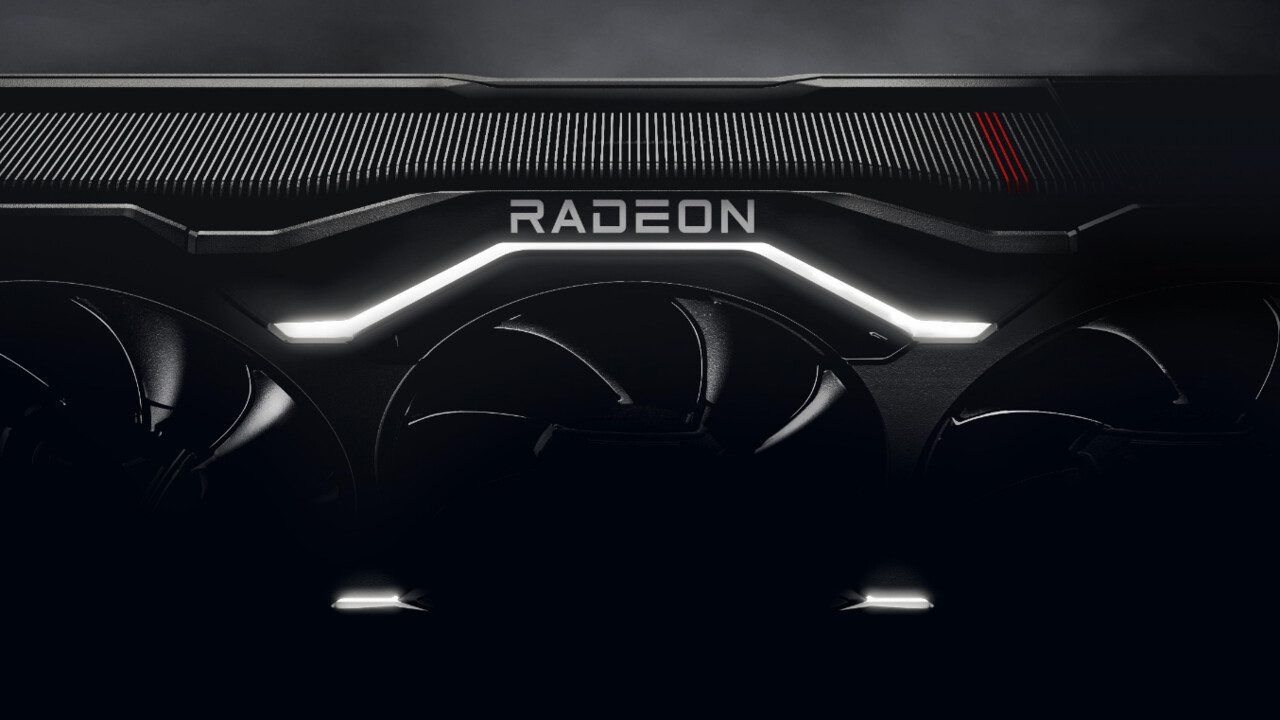
While Nvidia is likely to lift the curtain on the GeForce RTX 4000 in five days after months of wild speculation and leaks have gotten more concrete recently, AMD’s Radeon RX 7000 with RDNA 3 architecture has been pretty quiet again recently. . igor’s lab break the silence with the Radeon RX 7900 XT PCB schematic.
Drawing based on reliable sources
With a critical reference to the competition of Twitter leaks and the dispute that is repeatedly imposed between the parties involved igor’s lab a large number of reliable sources as the basis for the specially created drawing – the probability that what is shown corresponds to reality can be classified as high. The drawing “the lowest common denominator“From the photos, CAD drawings, and descriptions present. It should show a so-called custom design, although it should be close to the AMD reference.
Custom designs are the basis
The fact that three 8-pin PCIe connectors are soldered onto the circuit board fits the custom design character, whereas it was recently assumed that AMD would make do with two 8-pin connectors in reference designs. However, with two of these sockets, the power loss shouldn’t be much more than 300 watts (150 watts per 8-pin connection plus a maximum of 75 watts via PCIe) and custom designs should be higher, as they are doing it today.
In all likelihood, AMD still won’t rely on the new 12(+4)-pin 12VHPWR connector, which allows up to 600 watts through a single strand of cable. However, there is no certainty on this point. At Nvidia, both the Founders Edition and custom designs at the higher end of the performance range must be based on the new standard.
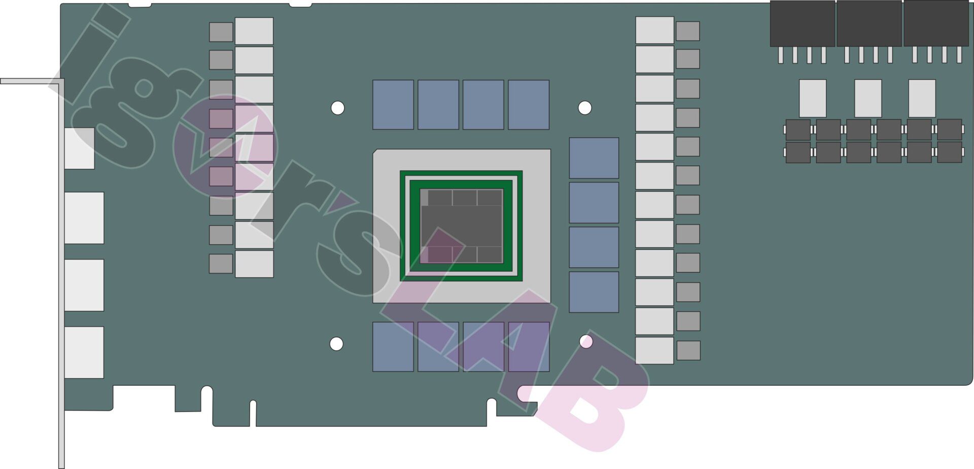
Radeon RX 7900 XT custom builds could be noisy igor’s lab up to 21 voltage converters, 16 of which provide the main voltages VDDC_GFX, memory, VDD_SOC and VDDCI in 8 duplicated phases, while five more provide the auxiliary voltages. This is not speculation, but is assured based on existing circuit designs.
Navi 31 with 6+1 chiplets
Furthermore, the schematic confirms the structure of Navi 31, already credibly traded in the rumor mill, consisting of a graphics compute die (processing unit) and six memory control dies (memory chip that includes Infinity Cache).
Of the six memory controllers, two 2 GB GDDR6 chips each need to be addressed via 32 bits each, resulting in 24 GB via a 384-bit interface. An HDMI port and three DisplayPort ports will be offered as connections.
Radeon RX 7000 will launch in 2022
AMD recently confirmed that RDNA 3 will launch later this year and showed off a working system with Ryzen 7000 GPUs and RDNA 3. However, AMD has yet to give exact dates or products.

Toni Morrison was a celebrated American author whose novels earned worldwide recognition for their depth, artistry, and cultural significance. Her influential works continue to inspire readers and writers across generations.