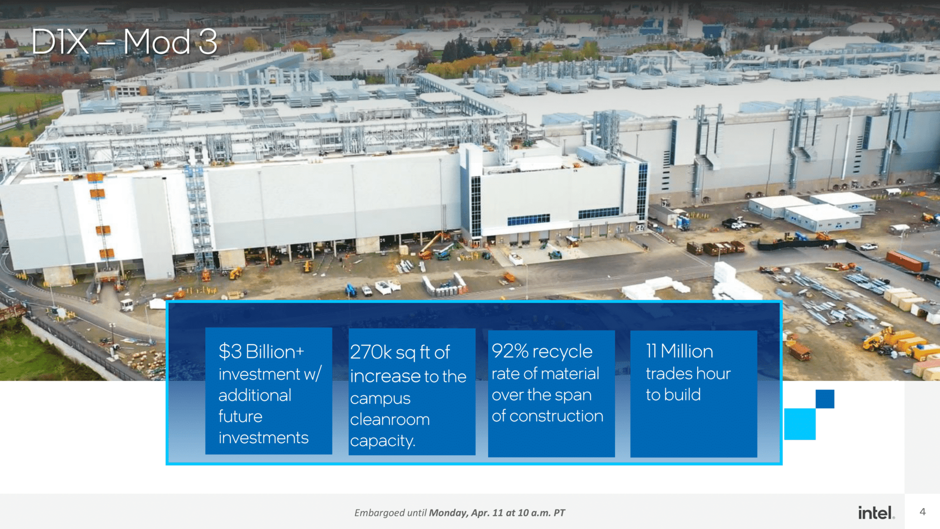
The Intel D1X research and development factory has been expanded with a new module. Among other things, the new EUV with high NA will be tested here. New machines require new buildings, so to speak, because they are bigger, heavier and, above all, taller. At the same time, Intel provided information on future developments.
Research and development again in the spotlight
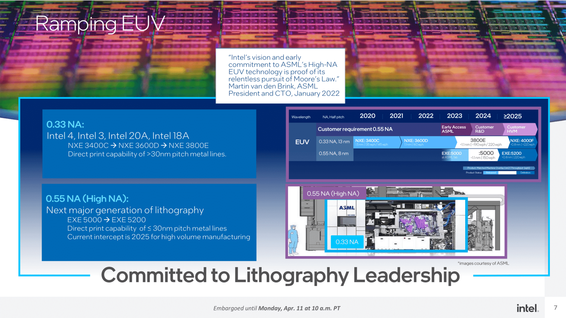
Investing $3 billion in a research and development factory is a staggering sum. The cleanroom area of the building called D1X is only increased by a little over 20 percent, but the new area has it all: In the new module, not only the upcoming classic EUV tools will be used, but also the cornerstone will be laid. for EUV with high NA. The fact that new buildings were necessary for this should also be a problem for Intel factories around the world in the future.
The new Mod3 from D1X is therefore probably also the model that will be implemented in future factories. After all, Intel is building several new plants in the coming years, and a complex in Magdeburg, Germany, was also recently confirmed.
-

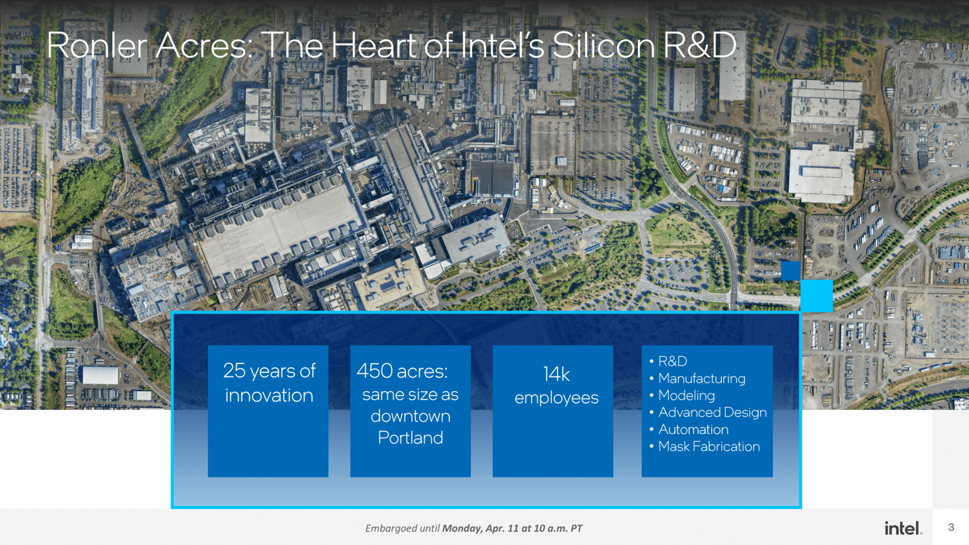
Intel Ronler Acres with a new building on the left (Image: Intel)
image one of 2
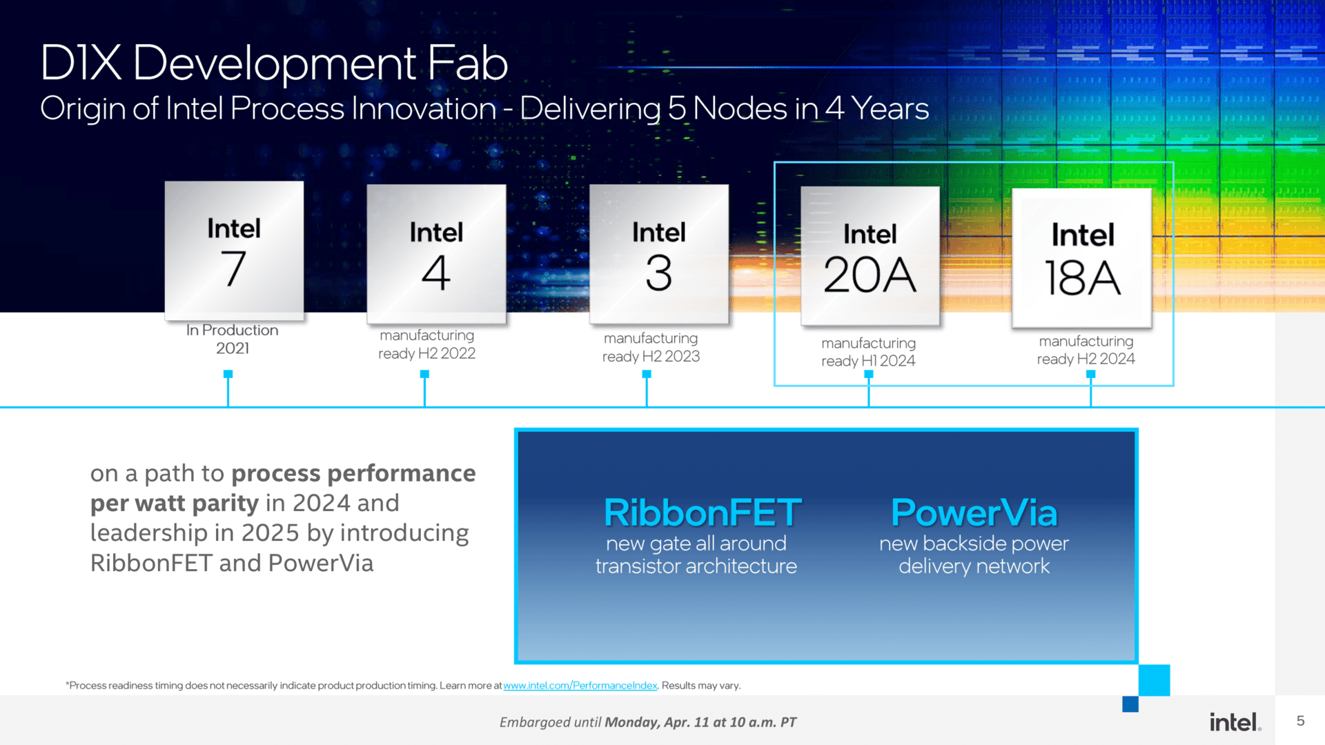
The factory will also test in the next few years if things don’t go as planned with High-NA EUV. Setting yourself up for failure and having a plan B up your sleeve was not Intel’s forte lately. According to Intel, the backup plan that has already been taken into account, which should also be able to implement the production steps with classic EUV exposure, will come into force in the near future. Potentially affected processors are mainly the Intel 20A, but also the Intel 18A, which was recently brought forward a bit and should be ready for series production in 2025, just six months after the Intel 20A. Today it is said that Intel could close the gap until 2026 with classic EUV lithography.
Intel sets up six years until a process has matured from the drawing board to serial production. The Component Research (CR) department is in charge for the first few years, with the Manufacturing Group only coming on board later.
-
From research and development to product (Image: Intel)
image one of 3
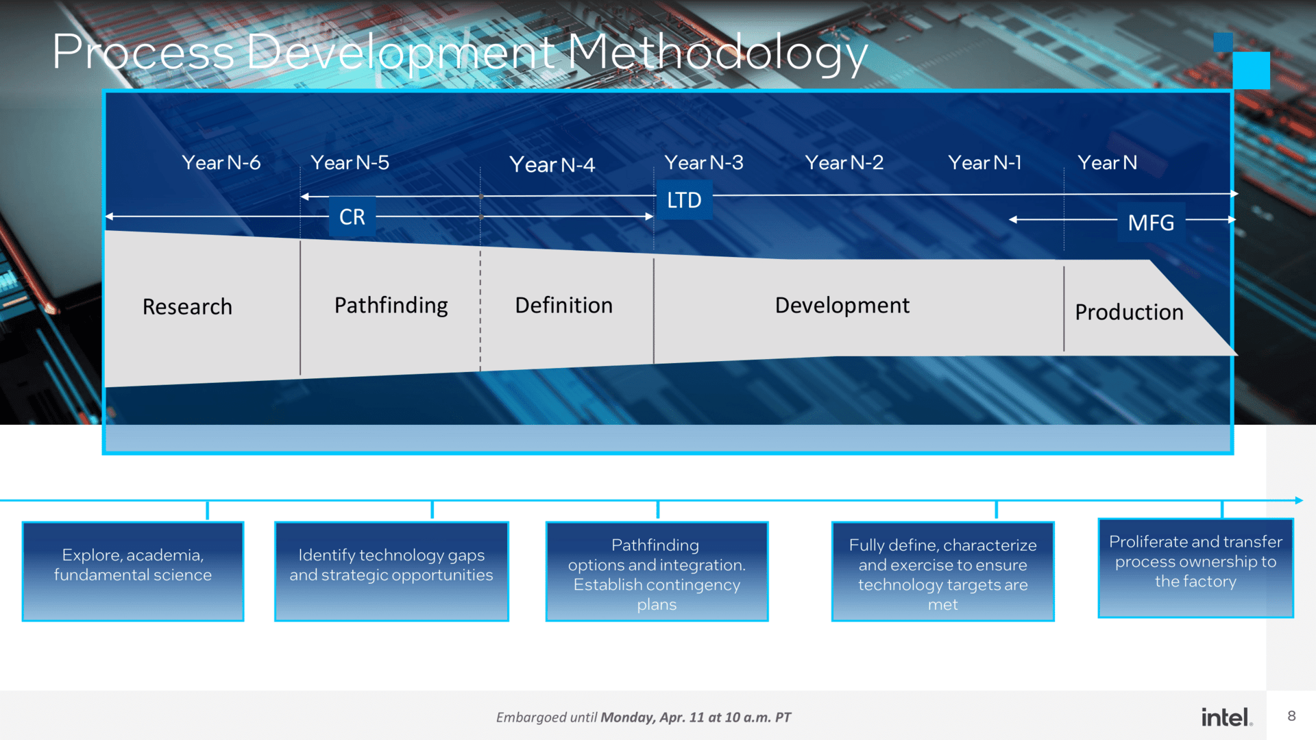
In the end, of course, it’s all about money. Here, Intel’s new CEO recently pulled out the checkbook and freed up more money to speed up implementation. However, cooperation with partners and the use of tools that are also used by other manufacturers deviate from the previous lone wolf approach. Much of what Intel has been doing in the factories is completely incompatible with other processes, and that starts with the design tools.
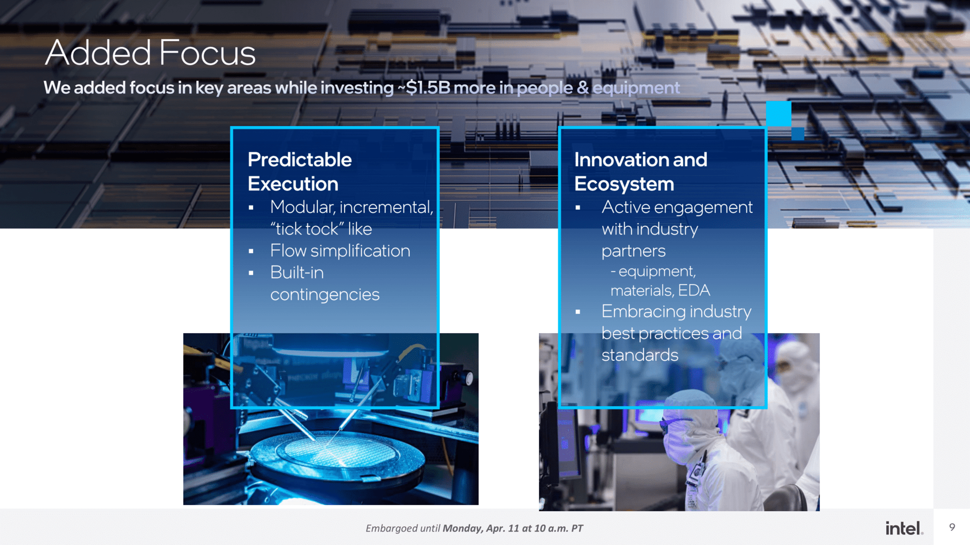
Don’t repeat the mistakes of the past
Speaking to the press last week, it was clear that Intel does not want to repeat the mistakes of the past, especially the ones that led to the 10nm nightmare. What the manufacturer publicly presents as an innovation for the future seems rather strange, because from the outside such mechanisms should have been effective in the past.
The fact that it didn’t exist explains well in hindsight why 10nm failed so badly on the first try and why it took Intel years to get back on track. In the end, the only thing that helped was removing half of the 10nm targets and starting from scratch. Intel has learned from this elsewhere, too: The tech roadmap timeline doesn’t mention a year.
Going forward, teams working on a process or technology for the new node will need to continue to support this technology in the future. There are also other teams that support and they don’t have to give up as soon as something new is planned. And with completely new processes, Intel no longer wants to implement everything at once in the future, which ultimately broke the 10nm neck on the first try.
So Intel has yet to manufacture in the now corrected and optimized 10nm, although it is now sold as Intel 7 in marketing. 7 years after the plan, which once foresaw a very optimistic introduction of 10nm in 2015. So what was it called in 2012 by Intel: “We know how to make 10nm chips” . The following years showed that this was not the case.
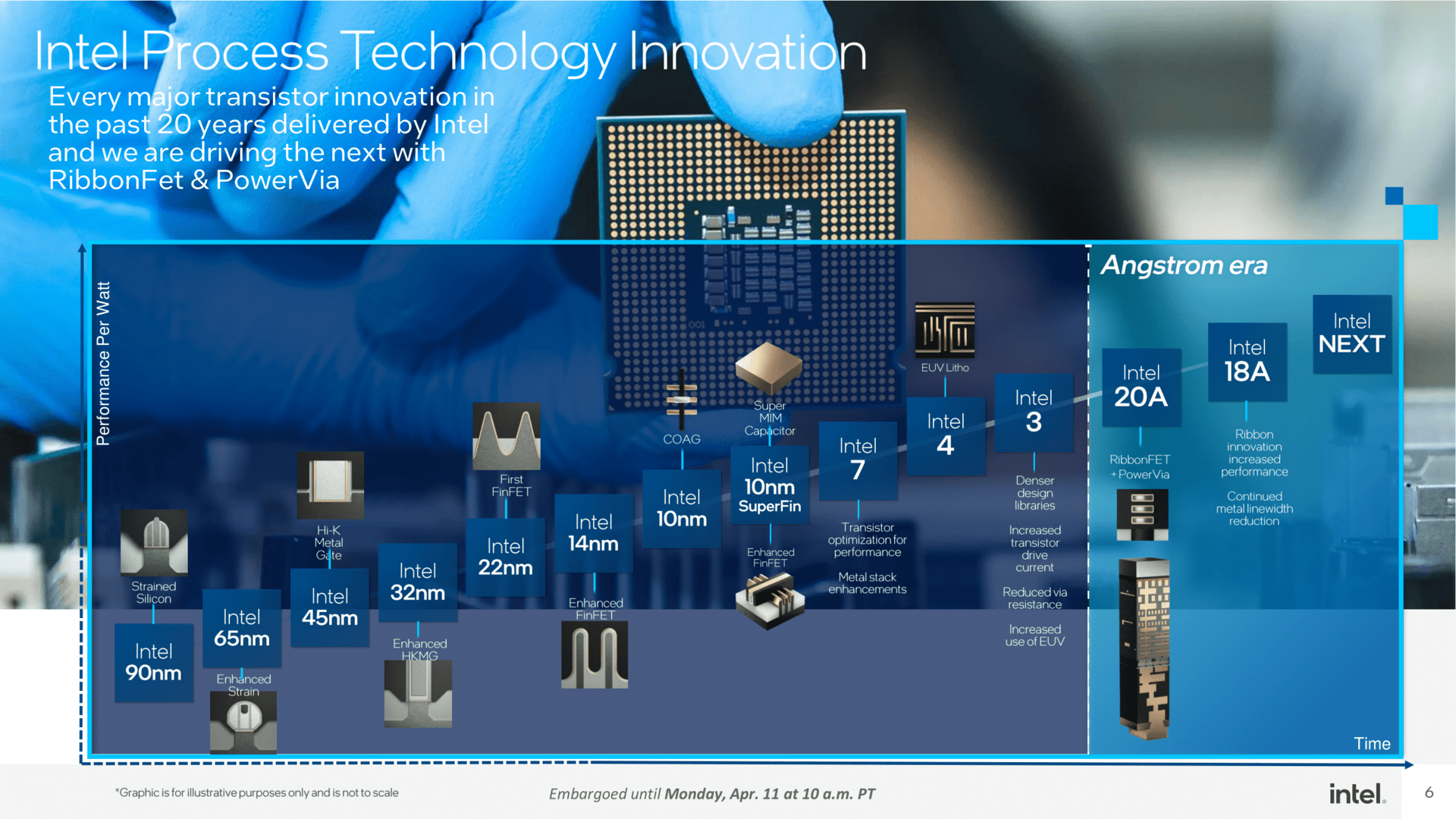
Internal intermediate process before PowerVia and GAA
This is best illustrated by the intermediate process that comes after Intel 3. It is not intended to produce any product, but is handled internally as an independent node. Intel is testing the new PowerVia on this with classic FinFETs. With this approach, a large potential source of error other than the PowerVia to be tested is almost impossible. FinFETs have been around for over a decade, it’s a proven technology. If problems arise, they should be attributed to PowerVia. Intel hopes that the solution can be found more quickly.
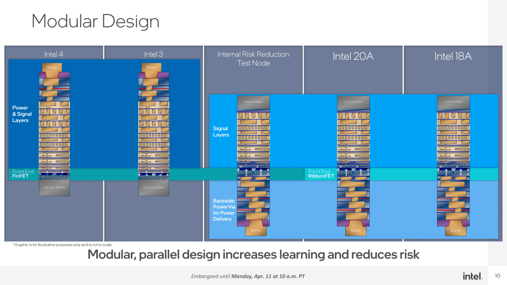
Once development is complete, the Gate-All-Around (GAA, Intel calls it the RibbonFET) is fed into the next node. The first process thus implemented is Intel 20A. But like many of the first of its kind, it will only be used in series for a short time based on current plans. Intel 18A should follow as an optimized variant within six months.
Ronler Acres becomes Gordon Moore Park
Intel properties in the US are often named after what used to be found on the ground. In Hillsboro, Oregon, for example, there is Hawthorn Farm and, even better known, Jones Farm, where not only technologies are developed, but also events are uploaded – ComputerBase has also been there several times.
The Ronler Acres complex with its factory buildings around D1C, D1D, and D1X and outbuildings used to follow this naming convention, but this is changing today. In homage to Intel’s greatest and most well-known personality, Gordon Moore, the entire complex is today renamed Gordon Moore Park at a ceremony.
Intel has a total of 22,000 employees in Hillsboro at four locations, and according to its own statements, more than US$52 billion has been invested in Oregon to date.
-
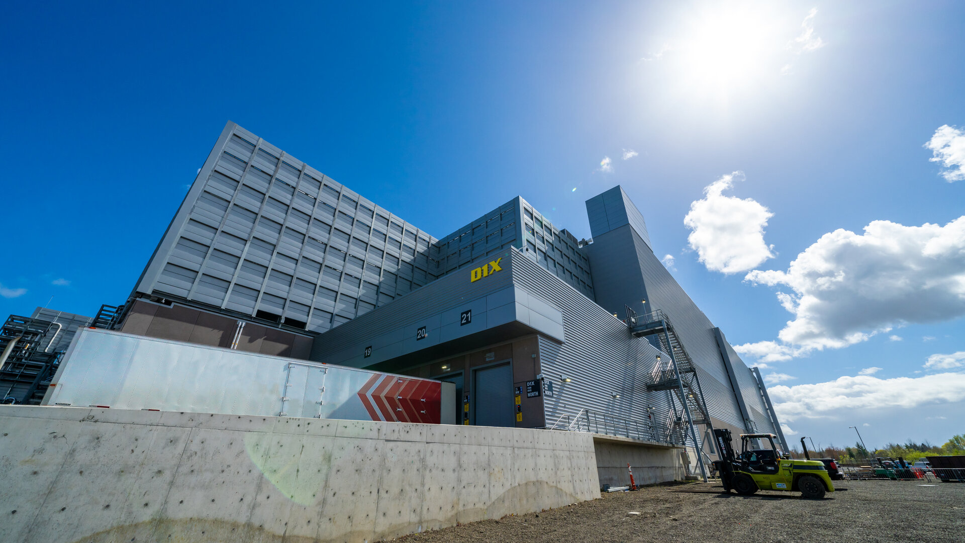
Intel D1X (Image: Intel)
image one of 3
ComputerBase received information about this article from Intel under NDA. The only requirement was the earliest possible publication date.

Introvert. Beer guru. Communicator. Travel fanatic. Web advocate. Certified alcohol geek. Tv buff. Subtly charming internet aficionado.